PN junction breakdown characteristics
In this article, we are going to learn a little deep about break down characteristics of PN Junction Diode and how “reverse break down” characteristics is put into practical applications. Before getting into the details, lets have a walk through our previous articles.
1. Understanding the PN Junction – is a great article to begin your learning curve about pn junction. In this article, we have clearly explained what is a pn junction and how is it formed.
2. PN Junction Characteristics– is another great article you must read to understand behavior of a PN junction under different conditions; say forward bias and reverse bias . This article will also help you understand why a PN junction is used in rectification applications.
Now lets comes to the essence of this article. “Break down” of a diode occurs during its reverse biased condition. We all know, under reverse bias the positive terminal of battery is connected to n side and the negative terminal of battery is connected to p side. As a result, electrons will be drawn towards the terminal of n side and holes will be draw towards terminal of p side. At this condition electron hole recombination will not happen and hence minority carrier movement is absent. This is the reason a diode is not conducting under reverse bias condition.
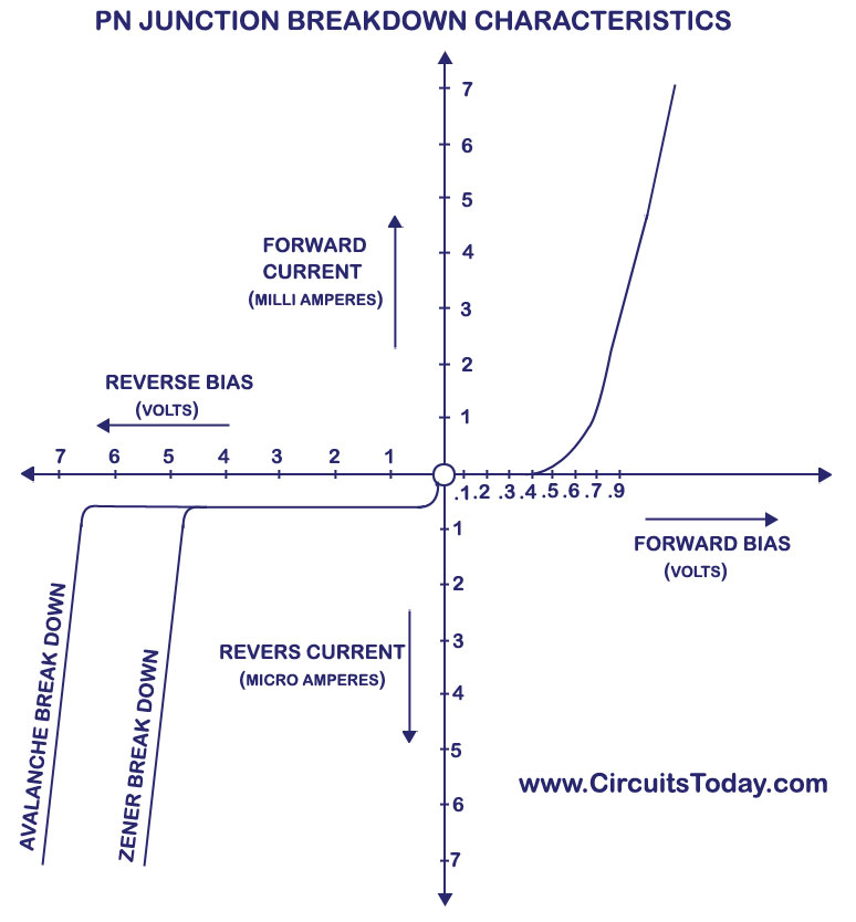
If we keep on increasing the applied reverse voltage, the depletion width will increase accordingly. At a point which we can call as “breakdown point”, the diode will get damaged. At this point, the diode behave more like a shorted wire and hence current flows through it easily. The internal resistance of diode at this stage is approximately near zero. According to Ohms Law, V = I/R and since resistance is very very low, current increases many folds with voltage. This is the reason we get a perpendicular line shoot in VI characteristics of reverse bias.
I hope you understood why break down of a diode occurs! It is because we increase the applied reverse voltage across the diode beyond a limit. Now let’s see how “break down” occurs!
PN Junction Breakdown
Electrical break down of any material (say metal, conductor, semiconductor or even insulator) can occur due to two different phenomena. Those two phenomena are 1) Zener breakdown and 2) Avalanche breakdown
These two phenomena are quite like a natural occurrence. It even applies to our daily life while lightning. We all know air is an insulator under normal conditions. But when lightning occurs (an extremely high voltage), it charges the air molecules nearby and charges get transferred via air medium. Now that’s a kind of electrical break down of an insulator. A similar kind of situation arises in zener and avalanche breakdown as well. Let see what’s it all about!
Zener Breakdown
When we increase the reverse voltage across the pn junction diode, what really happens is that the electric field across the diode junction increases (both internal & external). This results in a force of attraction on the negatively charged electrons at junction. This force frees electrons from its covalent bond and moves those free electrons to conduction band. When the electric field increases (with applied voltage), more and more electrons are freed from its covalent bonds. This results in drifting of electrons across the junction and electron hole recombination occurs. So a net current is developed and it increases rapidly with increase in electric field.
Zener breakdown phenomena occurs in a pn junction diode with heavy doping & thin junction (means depletion layer width is very small). Zener breakdown does not result in damage of diode. Since current is only due to drifting of electrons, there is a limit to the increase in current as well.
Avalanche Breakdown
Avalanche breakdown occurs in a pn junction diode which is moderately doped and has a thick junction (means its depletion layer width is high). Avalanche breakdown usually occurs when we apply a high reverse voltage across the diode (obviously higher than the zener breakdown voltage,say Vz). So as we increase the applied reverse voltage, the electric field across junction will keep increasing.
If applied reverse voltage is Va and the depletion layer width is d;then the generated electric field can be calculated as Ea =Va/d
This generated electric field exerts a force on the electrons at junction and it frees them from covalent bonds. These free electrons will gain acceleration and it will start moving across the junction with high velocity. This results in collision with other neighboring atoms. These collisions in high velocity will generate further free electrons. These electrons will start drifting and electron-hole pair recombination occurs across the junction. This results in net current that rapidly increases.
We learned that avalanche breakdown occurs at a voltage (Va) which is higher than zener breakdown voltage (Vz). The reason behind this is simple. We know, avalanche phenomena occurs in a diode which is moderately doped and junction width (say d) is high. A zener break down occurs in a diode with heavy doping and thin junction (here d is small). The electric field that occur due to applied reverse voltage (say V) can be calculated as E = V/d.
So in a Zener breakdown, the electric field necessary to break electrons from covalent bond is achieved with lesser voltage than in avalanche breakdown. The reason is thin depletion layer width. In avalanche breakdown, the depletion layer width is higher and hence much more reverse voltage has to be applied to develop the same electric field strength (necessary enough to break electrons free)

Comments
Post a Comment